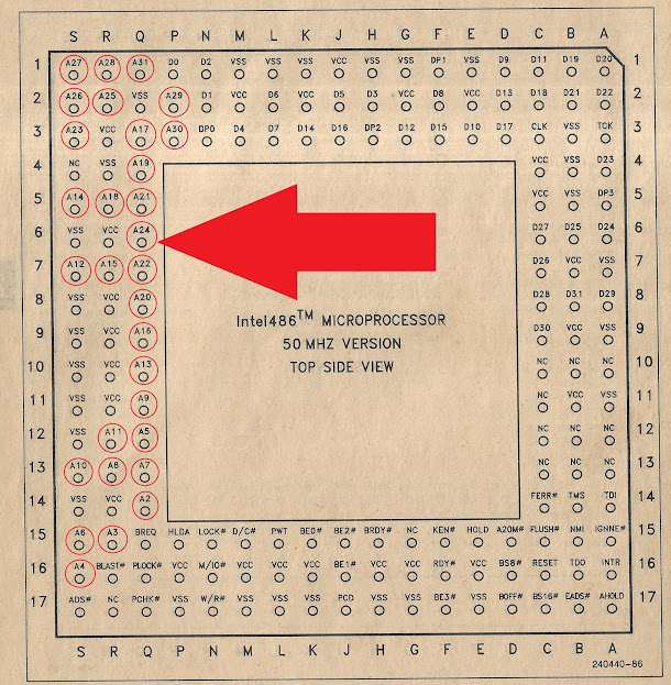
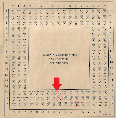
Pin Layout of Intel 486 Microprocessor
Pin Layout of Intel 486 Microprocessor
1. CLOCK, Symbol : CLK and Type : Input :-
CLK provides the fundamental timing and the internal operating frequency for the Intel486 microprocessor. All external timing parameters are specified with respect to the rising edge of CLK.
The Intel486 microprocessor can operate over a wide frequency range but CLK's frequency cannot change rapidly while RESET pin is Inactive.
CLK's frequency must be stable for proper chip operation since a single edge CLK is used internally to generate two phases. CLK only needs TTL levels for proper operation.
2. ADDRESS BUS, Symbol : A31-A4 and Type : Input-Output, Symbol : A2-A3 and Type : Output :-
A31-A2 are the address lines of the microprocessor. A31-A2, together with the byte enables BE0#-BE3#, define the physical area of memory or input/output space accessed. Address lines A31-A4 are used to drive addresses into the microprocessor to perform cache line invalidations.
A31-A2 and BE0#-BE3# form the address bus and provide physical memory and I/O port addresses. A31-A2 identify addresses to a 4-byte location. BE0#-BE3# identify which bytes within the 4-byte location are involved in the current transfer.
Addresses are driven back into the Intel486 microprocessor over A31-A4 during cache line invalidations. The address lines are active HIGH. when used as inputs into the processor, A31-A4 must meet the setup and hold times, t22 and t23 . A31-A2 are not driven during bus or address hold.
BE0#-BE3# can be decoded to generate A0, A1 and BHE# signals used in 8- and 16-bit systems.
3. ADDRESS BUS, Symbol : BE0#-BE3# and Type : Output :-
The byte enable signals indicate active bytes during read and write cycles. It means, the byte enable outputs, BE0#-BE3#, determine which bytes must be driven valid for read and write cycles to external memory.
During the first cycle of a cache fill, the external system should assume that all byte enables are active.
BE3# applies to D24-D31
BE2# applies to D16-D23
BE1# applies to D8-D15
BE0# applies to D0-D7
BE0#-BE3# are active LOW and are not driven during bus hold.
4. DATA BUS, Symbol : D31-D0 and Type : Input/Output :-
These are the data lines for the Intel486 microprocessor. These are bidirectional lines, D31-D0, form the data bus for the Intel486 microprocessor. Lines D0-D7 define the least significant byte of the data bus while lines D24-D31 define the most significant byte of the data bus.
Data transfers to 8- or 16-bit devices is possible using the data bus sizing feature controlled by the BS8# or BS16# input pins.


Comments
Post a Comment